News Details
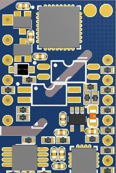
PCB design: "How to put it" and "How to connect"

“The first time to understand the domestic and international semiconductor, IC, electronics industry dynamics, original factory dynamics, market conditions, industry opportunities, policy directions and other information should not be missed”
PCB design is complicated, and various unexpected factors frequently affect the achievement of the overall solution. How can we tame the scattered parts with different personalities? How can I draw a neat, efficient and reliable PCB? Let us check it out today.
The PCB design seems to be complicated. It is necessary to consider the direction of various signals and the transmission of energy. The distress caused by interference and heat is also always present. But in fact, the summary is very clear and can be started from two aspects:
To put it bluntly, it is: "How to put it" and "How to connect."
Does it sound very easy? Let us first sort out the "how to put":
1. Follow the layout principle of “first big and then small, first difficult and easy”, that is, important unit circuits and core components should be prioritized. This is the same as eating a buffet: the appetite of the buffet is limited to pick the favorite food, and the PCB space is limited to pick the important pendulum.
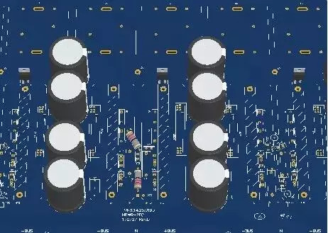
2. The layout should refer to the principle block diagram, and arrange the main components according to the main signal flow direction of the board. The layout should try to meet the following requirements: the total connection is as short as possible, and the key signal line is the shortest; the decoupling capacitor should be placed as close as possible to the power supply pin of the IC, and the loop formed between the power supply and the ground should be the shortest; Run the road to prevent accidents on the road.
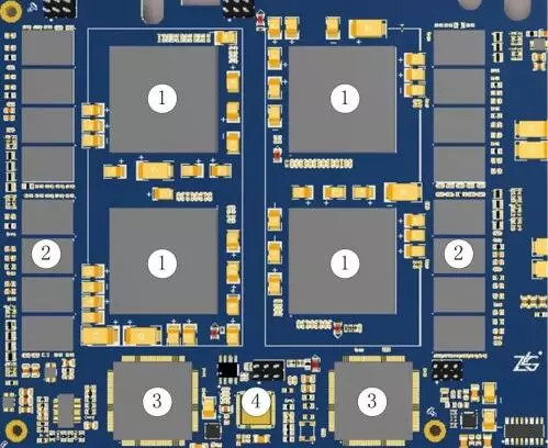
3. The arrangement of components should be easy to debug and repair, that is, there should be no large components around the small components, and there must be enough space around the components to be debugged.
4. The same structural circuit part, adopt the "symmetric" standard layout as much as possible; optimize the layout according to the standard of uniform distribution, balance of center of gravity and beautiful layout.
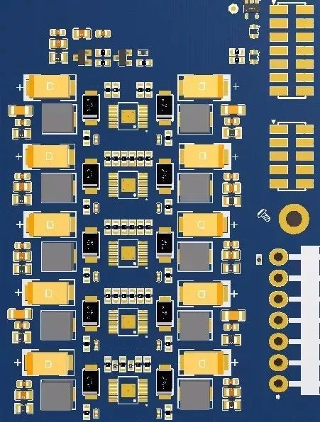
5. The same type of plug-in components should be placed in one direction in the X or Y direction. The same type of polar discrete components must also strive to be consistent in the X or Y direction for ease of production and inspection.
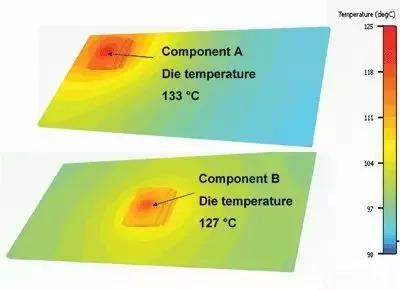
6. The heating elements should be evenly distributed in order to facilitate the heat dissipation of the single board and the whole machine. Temperature sensitive components other than the temperature detecting components should be kept away from the components with large heat generation.
7. The high voltage, high current signal and the small current, the low voltage weak signal are completely separated; the analog signal is separated from the digital signal; the high frequency signal is separated from the low frequency signal; the interval of the high frequency component is sufficient. When placing components, it should be considered that devices using the same power supply should be placed together as much as possible to facilitate future power separation.
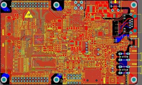
The above is the main consideration for the "how to put" layout. And the "how to connect" is relatively more complicated, in general:
Key signal line priority: simulate key signal priority routing such as small signal, high speed signal, clock signal and synchronization signal;
Density priority principle: Start wiring from the most complex devices connected on the board. Start wiring from the densest area of the board connection.
CONTACT US
- Tel:
- +86-574-62792283
- Fax:
- +86-574-22229987
- Email:
- ben@zonbo.net
- Add:
- NO.73, FENGMING ROAD, YUYAO CITY, ZHEJIANG PROVINCE,CHINA